
Via Fill Pastes from San-ei Kagaku

Minimal Z-Axis expansion under stress allows intricate build-up designs
Excellent paste hardness after cure enables flat pads after sanding
Features:
IR-6P series of pastes are ideal pastes for all circuit board applications, including computing, telecom, industrial, networking, MIL, aerospace. The pastes are economic, very simple to process with features, such as single step cure, excellent fill performance, ease of sanding, and have very reliable final performance properties.
The IR-10F series was designed for very high-end circuit board applications in mind. The material toughness is unrivaled with respect to final performance properties. Due to this excellent performance, this paste has become a standard in the North American market for high-end, long term performance applications. The combination of an ideal Tg, modulus and CTE values enables this paste to usually outperform all others when longevity material property tests are performed.
Gap Fill Pastes from San-ei Kagaku
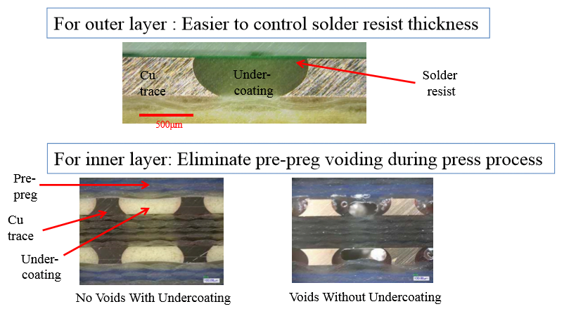
Gap fill used on an outer layer and then planarized to create a completely level surface, even with the Cu traces, regardless of the topography